- 您现在的位置:买卖IC网 > Sheet目录2004 > LTC1746IFW#TRPBF (Linear Technology)IC ADC 14BIT 25MSPS LP 48TSSOP
15
LTC1746
1746f
APPLICATIO S I FOR ATIO
WU
UU
Input Range
The input range can be set based on the application. For
oversampled signal processing in which the input fre-
quency is low (<10MHz), the largest input range will
provide the best signal-to-noise performance while main-
taining excellent SFDR. For high input frequencies
(>10MHz), the 2V range will have the best SFDR perfor-
mance but the SNR will degrade by 3.5dB. See the Typical
Performance Characteristics section.
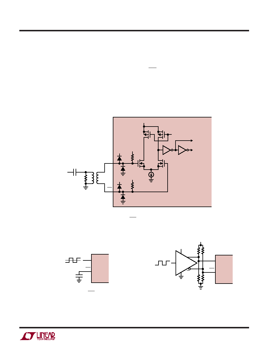
Driving the Encode Inputs
The noise performance of the LTC1746 can depend on the
encode signal quality as much as on the analog input. The
ENC/ENC inputs are intended to be driven differentially,
primarily for noise immunity from common mode noise
sources. Each input is biased through a 6k resistor to a 2V
bias. The bias resistors set the DC operating point for
transformer coupled drive circuits and can set the logic
threshold for single-ended drive circuits.
VDD
LTC1746
1746 F07
BIAS
VDD
5V
ENC
ANALOG INPUT
2V BIAS
1:4
0.1
F
CLOCK
INPUT
50
6k
TO INTERNAL
ADC CIRCUITS
Figure 7. Transformer Driven ENC/ENC with Equivalent Encode Input Circuit
1746 F08a
ENC
2V
VTHRESHOLD = 2V
ENC
0.1
F
LTC1746
1746 F08b
ENC
130
3.3V
130
D0
Q0
MC100LVELT22
LTC1746
83
83
Figure 8a. Single-Ended ENC Drive,
Not Recommended for Low Jitter
Figure 8b. ENC Drive Using a CMOS-to-PECL Translator
发布紧急采购,3分钟左右您将得到回复。
相关PDF资料
LTC1747IFW#PBF
IC ADC 12BIT 80MSPS 48-TSSOP
LTC1748CFW#TRPBF
IC ADC 14BIT 80MSPS 48-TSSOP
LTC1749IFW#PBF
IC ADC 12BIT 80MSPS SMPL 48TSSOP
LTC1750IFW#PBF
IC ADC 14BIT 80MSPS SMPL 48TSSOP
LTC1799HS5#TRPBF
IC OSC SILICON 33MHZ TSOT23-5
LTC1821ACGW
IC D/A CONV 16BIT PRECISE 36SSOP
LTC1851CFW
IC ADC 12BIT 1.25MSPS 48-TSSOP
LTC1853IFW#TRPBF
IC A/D CONV 8CH 12BIT 48-TSSOP
相关代理商/技术参数
LTC1747CFW
功能描述:IC ADC 12BIT 80MSPS 48-TSSOP RoHS:否 类别:集成电路 (IC) >> 数据采集 - 模数转换器 系列:- 标准包装:1 系列:- 位数:14 采样率(每秒):83k 数据接口:串行,并联 转换器数目:1 功率耗散(最大):95mW 电压电源:双 ± 工作温度:0°C ~ 70°C 安装类型:通孔 封装/外壳:28-DIP(0.600",15.24mm) 供应商设备封装:28-PDIP 包装:管件 输入数目和类型:1 个单端,双极
LTC1747CFW#PBF
功能描述:IC ADC 12BIT 80MSPS 48-TSSOP RoHS:是 类别:集成电路 (IC) >> 数据采集 - 模数转换器 系列:- 产品培训模块:Lead (SnPb) Finish for COTS
Obsolescence Mitigation Program 标准包装:2,500 系列:- 位数:12 采样率(每秒):3M 数据接口:- 转换器数目:- 功率耗散(最大):- 电压电源:- 工作温度:- 安装类型:表面贴装 封装/外壳:SOT-23-6 供应商设备封装:SOT-23-6 包装:带卷 (TR) 输入数目和类型:-
LTC1747CFW#TR
功能描述:IC ADC SMPL 12BIT 80MSPS 48TSSOP RoHS:否 类别:集成电路 (IC) >> 数据采集 - 模数转换器 系列:- 标准包装:1 系列:- 位数:14 采样率(每秒):83k 数据接口:串行,并联 转换器数目:1 功率耗散(最大):95mW 电压电源:双 ± 工作温度:0°C ~ 70°C 安装类型:通孔 封装/外壳:28-DIP(0.600",15.24mm) 供应商设备封装:28-PDIP 包装:管件 输入数目和类型:1 个单端,双极
LTC1747CFW#TRPBF
功能描述:IC ADC 12BIT 80MSPS 48-TSSOP RoHS:是 类别:集成电路 (IC) >> 数据采集 - 模数转换器 系列:- 产品培训模块:Lead (SnPb) Finish for COTS
Obsolescence Mitigation Program 标准包装:2,500 系列:- 位数:12 采样率(每秒):3M 数据接口:- 转换器数目:- 功率耗散(最大):- 电压电源:- 工作温度:- 安装类型:表面贴装 封装/外壳:SOT-23-6 供应商设备封装:SOT-23-6 包装:带卷 (TR) 输入数目和类型:-
LTC1747IFW
功能描述:IC ADC SMPL 12BIT 80MSPS 48TSSOP RoHS:否 类别:集成电路 (IC) >> 数据采集 - 模数转换器 系列:- 标准包装:1 系列:- 位数:14 采样率(每秒):83k 数据接口:串行,并联 转换器数目:1 功率耗散(最大):95mW 电压电源:双 ± 工作温度:0°C ~ 70°C 安装类型:通孔 封装/外壳:28-DIP(0.600",15.24mm) 供应商设备封装:28-PDIP 包装:管件 输入数目和类型:1 个单端,双极
LTC1747IFW#PBF
功能描述:IC ADC 12BIT 80MSPS 48-TSSOP RoHS:是 类别:集成电路 (IC) >> 数据采集 - 模数转换器 系列:- 产品培训模块:Lead (SnPb) Finish for COTS
Obsolescence Mitigation Program 标准包装:2,500 系列:- 位数:12 采样率(每秒):3M 数据接口:- 转换器数目:- 功率耗散(最大):- 电压电源:- 工作温度:- 安装类型:表面贴装 封装/外壳:SOT-23-6 供应商设备封装:SOT-23-6 包装:带卷 (TR) 输入数目和类型:-
LTC1747IFW#TR
功能描述:IC ADC SMPL 12BIT 80MSPS 48TSSOP RoHS:否 类别:集成电路 (IC) >> 数据采集 - 模数转换器 系列:- 标准包装:1 系列:- 位数:14 采样率(每秒):83k 数据接口:串行,并联 转换器数目:1 功率耗散(最大):95mW 电压电源:双 ± 工作温度:0°C ~ 70°C 安装类型:通孔 封装/外壳:28-DIP(0.600",15.24mm) 供应商设备封装:28-PDIP 包装:管件 输入数目和类型:1 个单端,双极
LTC1747IFW#TRPBF
功能描述:IC ADC 12BIT 80MSPS 48-TSSOP RoHS:是 类别:集成电路 (IC) >> 数据采集 - 模数转换器 系列:- 产品培训模块:Lead (SnPb) Finish for COTS
Obsolescence Mitigation Program 标准包装:2,500 系列:- 位数:12 采样率(每秒):3M 数据接口:- 转换器数目:- 功率耗散(最大):- 电压电源:- 工作温度:- 安装类型:表面贴装 封装/外壳:SOT-23-6 供应商设备封装:SOT-23-6 包装:带卷 (TR) 输入数目和类型:-